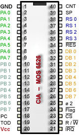
Der C64 hat zwei Bausteine des Typs MOS 6526; ersterer DC00h-DCFFh, zweiterer DD00h-DDFFh.
| CIA 1 |
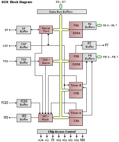
| DC00 | Data Port A (Keyboard, Joystick, Paddles, Light-Pen)
7-0 Write Keyboard Column Values for Keyboard Scan
7-6 Read Paddles on Port A / B (01 = Port A, 10 = Port B)
4 Joystick A Fire Button: 1 = Fire
3-2 Paddle Fire Buttons
3-0 Joystick A Direction (0-15) |
| DC01 | Data Port B (Keyboard, Joystick, Paddles): Game Port 1
7-0 Read Keyboard Row Values for Keyboard Scan
7 Timer B Toggle/Pulse Output
6 Timer A: Toggle/Pulse Output
4 Joystick 1 Fire Button: 1 = Fire
3-2 Paddle Fire Buttons
3-0 Joystick 1 Direction |
| DC02 | Data Direction Register - Port A |
| DC03 | Data Direction Register - Port B |
| DC04 | Timer A: Low-Byte |
| DC05 | Timer A: High-Byte |
| DC06 | Timer B: Low-Byte |
| DC07 | Timer B: High-Byte |
| DC08 | Time-of-Day Clock: 1/10 Seconds |
| DC09 | Time-of-Day Clock: Seconds |
| DC0A | Time-of-Day Clock: Minutes |
| DC0B | Time-of-Day Clock: Hours + AM/PM Flag (Bit 7) |
| DC0C | Synchronous Serial I/O Data Buffer |
| DC0D | CIA Interrupt Control Register (Read IRQs/Write Mask)
7 IRQ Flag (1 = IRQ Occurred) / Set-Clear Flag
4 FLAG1 IRQ (Cassette Read / Serial Bus SRQ Input)
3 Serial Port Interrupt
2 Time-of-Day Clock Alarm Interrupt
1 Timer B Interrupt
0 Timer A Interrupt |
| DC0E | CIA Control Register A
7 Time-of-Day Clock Frequency: 1 = 50 Hz, 0 = 60 Hz
6 Serial Port I/O Mode Output, 0 = Input
5 Timer A Counts: 1 = CNT Signals, 0 = System 02 Clock
4 Force Load Timer A: 1 = Yes
3 Timer A Run Mode: 1 = One-Shot, 0 = Continuous
2 Timer A Output Mode to PB6: 1 = Toggle, 0 = Pulse
1 Timer A Output on PB6: 1 = Yes, 0 = No
0 Start/Stop Timer A: 1 = Start, 0 = Stop |
| DC0F | CIA Control Register B
7 Set Alarm/TOD-Clock: 1 = Alarm, 0 = Clock
6-5 Timer B Mode Select:
00 = Count System 02 Clock Pulses
01 = Count Positive CNT Transitions
10 = Count Timer A Underflow Pulses
11 = Count Timer A Underflows While CNT Positive
4-0 Same as CIA Control Reg. A - for Timer B |
| |
| CIA 2 |
| DD00 | Data Port A (Serial Bus, RS-232, VIC Memory Control)
7 Serial Bus Data Input
6 Serial Bus Clock Pulse Input
5 Serial Bus Data Output
4 Serial Bus Clock Pulse Output
3 Serial Bus ATN Signal Output
2 RS-232 Data Output (User Port)
1-O VIC Chip System Memory Bank Select (Default = 11) |
| DD01 | Data Port B (User Port, RS-232)
7 User / RS-232 Data Set Ready
6 User / RS-232 Clear to Send
5 User
4 User / RS-232 Carrier Detect
3 User / RS-232 Ring Indicator
2 User / RS-232 Data Terminal Ready
1 User / RS-232 Request to Send
0 User / RS-232 Received Data |
| DD02 | Data Direction Register - Port A |
| DD03 | Data Direction Register - Port B |
| DD04 | Timer A: Low-Byte |
| DD05 | Timer A: High-Byte |
| DD06 | Timer B: Low-Byte |
| DD07 | Timer B: High-Byte |
| DD08 | Time-of-Day Clock: 1/10 Seconds |
| DD09 | Time-of-Day Clock: Seconds |
| DD0A | Time-of-Day Clock: Minutes |
| DD0B | Time-of-Day Clock: Hours + AM/PM Flag (Bit 7) |
| DD0C | Synchronous Serial I/O Data Buffer |
| DD0D | CIA Interrupt Control Register (Read NMls/Write Mask)
7 NMI Flag (1 = NMI Occurred) / Set-Clear Flag
4 FLAG1 NMI (User/RS-232 Received Data Input)
3 Serial Port Interrupt
1 Timer B Interrupt
0 Timer A Interrupt |
| DD0E | CIA Control Register A
7 Time-of-Day Clock Frequency: 1 = 50 Hz, 0 = 60 Hz
6 Serial Port I/O Mode Output, 0 = Input
5 Timer A Counts: 1 = CNT Signals, 0 = System 02 Clock
4 Force Load Timer A: 1 = Yes
3 Timer A Run Mode: 1 = One-Shot, 0 = Continuous
2 Timer A Output Mode to PB6: 1 = Toggle, 0 = Pulse
1 Timer A Output on PB6: 1 = Yes, 0 = No
0 Start/Stop Timer A: 1 = Start, 0 = Stop |
| DD0F | CIA Control Register B
7 Set Alarm/TOD-Clock: 1 = Alarm, 0 = Clock
6-5 Timer B Mode Select:
00 = Count System 02 Clock Pulses
01 = Count Positive CNT Transitions
10 = Count Timer A Underflow Pulses
11 = Count Timer A Underflows While CNT Positive
4-0 Same as CIA Control Reg. A - for Timer B |