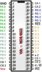
Die C1541-Floppy besitzt zwei Bausteine des Typs MOS 6522 wovon ersterer (ab 1800hex) zur Datenübertragung mit dem C-64 dient, zweiter (ab 1C00hex) zur Ansteuerung der Motoren und Schreib-/Leseköpfe.
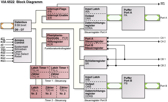
| Reg. | Beschreibung |
| 0 | Register B |
| 1 | Register A |
| 2 | Data Direction Register B: LOW=Input, HIGH=Output |
| 3 | Data Direction Register A: LOW=Input, HIGH=Output |
| 4 | Timer 1 Count Value (LOW Order Counter) |
| 5 | Timer 1 Count Value (HIGH Order Counter) |
| 6 | Timer 1 Count Value (LOW Order Latch) |
| 7 | Timer 1 Count Value (HIGH Order Latch) |
| 8 | Timer 2 Count Value (LOW Order Latch/Counter) |
| 9 | Timer 2 Count Value (HIGH Order Latch/Counter) |
| A | Shift Register (links- oder rechts-rotierend |
| B | Auxiliary Control Register
Bit 6-7: Timer 1 Control:
00: Timer wird geladen (PB7=Disable)
01: Continuous Interrupt (PB7=Disable)
10: Timer 1 wird gelden (PB7="One Shot Output")
11: Continuous Interrupt (PB7="Square Wave Output")
Bit 5: Timer 2 Control: LOW=Interrupt, HIGH=PB6
Bit 2-4: Shift Register Control:
000: Disable
001: Shift wird von Timer 2 kontrolliert
010: Shift wird vom Systemtakt kontrolliert
011: Shift wird von Externem Takt kontrolliert
100: Shift läuft frei, angelehnt an Timer 2
101: Shift vom Timer 2 kontrolliert
110: Shift vom Systemtakt kontrolliert
111: Shift von externem Takt kontrolliert
Bit 1: PB bei LOW=Dissable, HIGH=Enable
Bit 0: PA bei LOW=Dissable, HIGH=Enable |
| C | Peripheral Control Register
Bit 5-7: CB2 Control
000: Input neg. active edge
001: Independent Interrupt/Input negatve edge
010: Input pos. active edge
011: Independent Interrupt/Input postive edge
100: Handshake Output
101: Pulse Output
110: Low Output
111: High Output
Bit 4: CB1 Interrupt Control (LOW=neg. Active edge, HIGH=pos. Active edge)
Bit 1-3: CA2 Control
Bedeutung gleich wie bei Bit 5-7
Bit 0: CA1 Interrupt Control (LOW=neg. Active edge, HIGH=pos. Active edge) |
| D | Interrupt Flag Register
Bit 7: IRQ LOW=clear Interrupt, HIGHT= Interrupt enable
Bit 6: Timeout Timer 1
Bit 5: Timerout Timer 2
Bit 4: CB1 Active Edge
Bit 3: CB2 Active Edge
Bit 2: acht Shifts beendet
Bit 1: CA1 Active Edge
Bit 0: CA2 Active Edge |
| E | Interrupt Enable Register (LOW=Disable, HIGH=Enable)
Bit 7: Set/Clear
Bit 6: Timer 1
Bit 5: Timer 2
Bit 4: CB 1
Bit 3: CB 2
Bit 2: Shift Register
Bit 1: CA 1
Bit 0: CA 2 |
| F | Register A (ohne Handschake) |